Intrinsic Carrier Concentration Of Silicon At 300k
Juapaving
Mar 17, 2025 · 6 min read
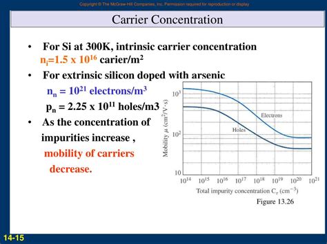
Table of Contents
Intrinsic Carrier Concentration of Silicon at 300K: A Deep Dive
Understanding the intrinsic carrier concentration (nᵢ) of silicon at 300K (room temperature) is fundamental to semiconductor physics and device design. This parameter dictates the number of electrons and holes present in pure silicon at thermal equilibrium, directly impacting its electrical conductivity and behavior in electronic devices. This article will delve deep into the concept, exploring its calculation, influencing factors, and practical implications.
What is Intrinsic Carrier Concentration (nᵢ)?
In a pure (intrinsic) semiconductor like silicon, the number of free electrons in the conduction band equals the number of holes in the valence band. This equality arises from the thermal generation of electron-hole pairs. At a given temperature, these thermally generated carriers are responsible for the material's intrinsic conductivity. nᵢ represents this concentration of electrons (or holes) in an intrinsic semiconductor. It’s a crucial parameter because it forms the basis for understanding doping and the behavior of extrinsic semiconductors.
At 300K (approximately room temperature), silicon's intrinsic carrier concentration is relatively low compared to metals, making it a suitable material for semiconductor devices. However, even this small concentration significantly affects its electrical properties.
Factors Affecting nᵢ in Silicon
Several factors influence the value of nᵢ at a given temperature, most importantly:
1. Temperature (T):
Temperature plays a dominant role. Higher temperatures provide more thermal energy, leading to an increased generation rate of electron-hole pairs. This results in a significantly higher nᵢ. The relationship between nᵢ and temperature is exponential, following the Arrhenius equation (explained later).
2. Bandgap Energy (E<sub>g</sub>):
The bandgap energy (E<sub>g</sub>) of silicon, which is the energy difference between the valence band and the conduction band, is another critical factor. A larger bandgap requires more energy to excite electrons from the valence band to the conduction band, resulting in a lower nᵢ at a given temperature. Silicon’s bandgap at 300K is approximately 1.12 eV.
3. Effective Mass of Electrons and Holes (m*<sub>n</sub>, m*<sub>p</sub>):
Electrons and holes don't behave exactly like free particles; their effective masses (m*<sub>n</sub> for electrons and m*<sub>p</sub> for holes) reflect their interaction with the crystal lattice. These effective masses influence the density of states in the conduction and valence bands, consequently affecting nᵢ. Heavier effective masses lead to lower nᵢ.
Calculating nᵢ for Silicon at 300K
The intrinsic carrier concentration can be calculated using the following equation derived from statistical thermodynamics:
nᵢ = √(N<sub>c</sub>N<sub>v</sub>) * exp(-E<sub>g</sub>/2kT)
Where:
- nᵢ is the intrinsic carrier concentration.
- N<sub>c</sub> is the effective density of states in the conduction band.
- N<sub>v</sub> is the effective density of states in the valence band.
- E<sub>g</sub> is the bandgap energy of silicon (approximately 1.12 eV at 300K).
- k is Boltzmann's constant (8.617 x 10<sup>-5</sup> eV/K).
- T is the absolute temperature in Kelvin (300K).
N<sub>c</sub> and N<sub>v</sub> are given by:
N<sub>c</sub> = 2(2πm<sub>n</sub>kT/h²)<sup>3/2</sup>*
N<sub>v</sub> = 2(2πm<sub>p</sub>kT/h²)<sup>3/2</sup>*
Where:
- m<sub>n</sub>* is the effective mass of electrons.
- m<sub>p</sub>* is the effective mass of holes.
- h is Planck's constant (6.626 x 10<sup>-34</sup> Js).
The values of m*<sub>n</sub> and m*<sub>p</sub> for silicon are not single, fixed numbers but depend on the crystallographic direction and the energy band structure. However, approximate values are often used for calculations, leading to an approximate value for nᵢ. Using typical values for silicon at 300K, the calculation yields an intrinsic carrier concentration on the order of 10<sup>10</sup> cm<sup>-3</sup>. This signifies that in a cubic centimeter of pure silicon at room temperature, approximately 10<sup>10</sup> electron-hole pairs are generated due to thermal energy.
Practical Implications of nᵢ
The intrinsic carrier concentration is not merely a theoretical concept; it has several crucial implications in semiconductor device physics and engineering:
1. Doping and Extrinsic Semiconductors:
Understanding nᵢ is essential for controlling the conductivity of silicon by doping. Doping introduces impurity atoms (either donors or acceptors) into the silicon lattice, significantly increasing the carrier concentration beyond nᵢ. This leads to either n-type (electron-rich) or p-type (hole-rich) semiconductors, crucial for creating transistors, diodes, and other semiconductor devices. The doping levels are typically orders of magnitude higher than nᵢ.
2. Semiconductor Device Performance:
The intrinsic carrier concentration directly affects the performance of semiconductor devices. For example, in a bipolar junction transistor, the base current is influenced by nᵢ, which in turn affects the transistor's gain and switching speed. Similarly, in a diode, the reverse saturation current is related to nᵢ.
3. Temperature Dependence of Semiconductor Devices:
Since nᵢ is highly temperature-dependent, the performance of semiconductor devices changes with temperature. This effect is often crucial in designing devices for various temperature ranges, and understanding the temperature-nᵢ relationship is necessary for accurate device modeling and simulation.
4. Material Purity:
The measured carrier concentration in a silicon sample can indicate its purity. A significantly higher concentration than the theoretical nᵢ at 300K suggests the presence of impurities and a departure from intrinsic behavior.
Approximations and Refinements
The calculation of nᵢ presented earlier employs several simplifications. For highly accurate calculations, refinements are necessary:
- More accurate effective mass values: Considering the anisotropy of the effective masses and energy-dependent variations can improve accuracy.
- Temperature dependence of E<sub>g</sub>: The bandgap energy itself has a slight temperature dependence, which can affect the nᵢ calculation.
- Non-parabolic band structure: The assumption of parabolic energy bands is an approximation; a more accurate treatment of the non-parabolic band structure can enhance precision.
Advanced Concepts and Applications
The intrinsic carrier concentration provides a foundation for understanding more complex phenomena in semiconductor physics:
- Carrier mobility: The intrinsic carrier mobility is affected by the scattering of carriers by phonons (lattice vibrations) and impurities. This mobility is linked to conductivity, which is directly related to nᵢ.
- Recombination and generation: Electron-hole recombination and generation rates are related to nᵢ, and understanding these processes is crucial for analyzing device behavior, particularly under non-equilibrium conditions.
- Photoconductivity: When exposed to light, silicon generates electron-hole pairs in excess of nᵢ, leading to photoconductivity. The magnitude of this photoconductivity depends on the balance between generation and recombination rates, both of which are indirectly related to nᵢ.
Conclusion
The intrinsic carrier concentration of silicon at 300K is a fundamental parameter influencing numerous aspects of semiconductor device physics and engineering. While a simplified calculation provides a reasonable estimate, advanced treatments accounting for the nuances of effective mass, band structure, and temperature dependence are necessary for high-precision applications. Understanding nᵢ is critical for designing, optimizing, and modeling semiconductor devices, ensuring their reliable operation across various temperature and environmental conditions. Its significance extends to diverse areas of semiconductor technology, highlighting its central role in this vital field. The accurate determination and application of this parameter remain essential for continued advancements in semiconductor device performance and functionality.
Latest Posts
Latest Posts
-
What Is The Least Common Multiple Of 24 And 12
Mar 17, 2025
-
Which Of The Following Is Not Associated With Animal Cells
Mar 17, 2025
-
How To Find The Inverse Of A Relation
Mar 17, 2025
-
Which Is The Order Of Airflow During Inhalation
Mar 17, 2025
-
Write 30 As A Product Of Prime Factors
Mar 17, 2025
Related Post
Thank you for visiting our website which covers about Intrinsic Carrier Concentration Of Silicon At 300k . We hope the information provided has been useful to you. Feel free to contact us if you have any questions or need further assistance. See you next time and don't miss to bookmark.
